07-Simulation and PCB layout
I. Introduction to RF PCB Layout
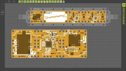
Figure: Microwave PCB
layout [www.x-microwave.com]
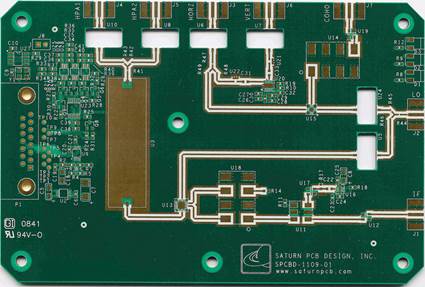
Figure: Microwave PCB before
mounting and soldering of components [www.saturnpcb.com]
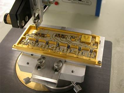
Figure: Microwave
multi-chip module in wire bond assembly [General Electronics Devices]
II. RF PCB Layout Fundamentals
https://www.raypcb.com/rf-pcb-design-layout-and-recommendations/
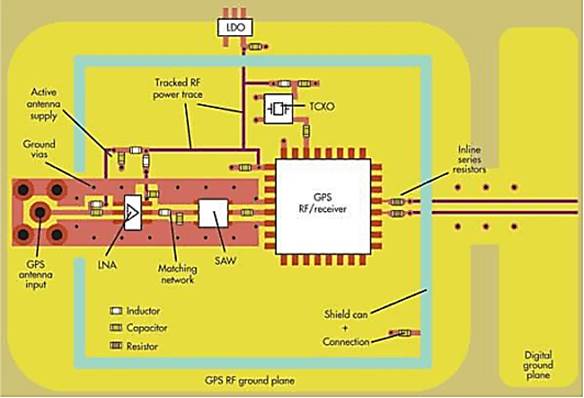
1. A simple RF PCB layout
example: a GPS receiver
2. IC input and output
lines
With specified Z0
Various forms of lines (micrstrip,
stripline, GCWP)
Bend mitering
Line layer change
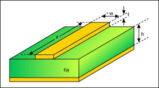
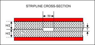
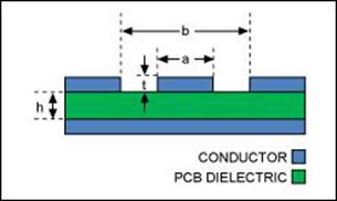
3. Line types
Microstrip line
Stripline
GCPW
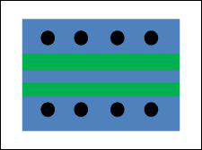
3. Via
fence for GCPW
- Via diameter: size
constraints
- Via spacing: < 0.25 ��
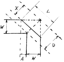
4. Bend mitering
- Circular bend: bending
radius > 3W
- Mitered bend
![]()
![]()
![]()
Online bend calculator: everythingRF, https://www.everythingrf.com/rf-calculators/microstrip-mitred-bend-calculator
- Bend drawing
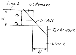
1. Make Line 1 and Line 2.
2. Find ������ è�۷��� �־��� ��� ���� �����κ��� H1, H2�� ���Ѵ�.
![]()
3. Remove T1 and T2 and add T0.