ICT083 Antenna
Design
Small Antennas
II. Lab
1. Short Dipole and Impedance Matching
Design frequency: 300 MHz
Wavelength: 1 m
Dipole length: 0.1 wavelength
Wire diameter: 0.001 wavelength
Feed gap: 0.001 wavelength
Wire material: Copper (conductivity 5.7 × 10⁷ S/m)
Simulation frequency range: 280-320 MHz
Impedance matching frequency: 300 MHz
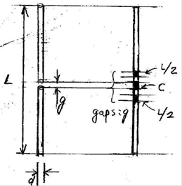
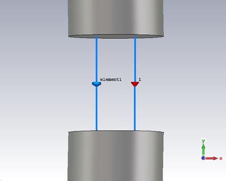
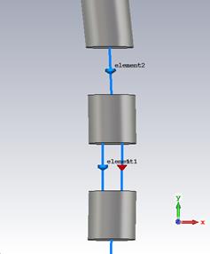
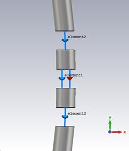
Figure: Short dipole and impedance matching. Inductors L/2 are
inserted in the dipole wire while the capacitor C is connected across the feed gap in parallel with the discrete
port.
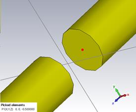
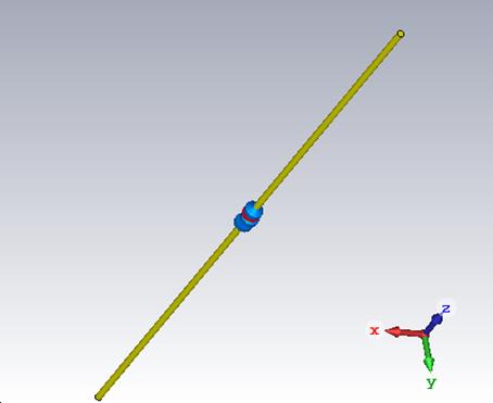
P1. Plot the antenna geometry
Dipole center at
(x, y, z) = (0, 0, 0)
Dipole axis in the z direction
f =300 MHz
λ = 300/0.3 = 1000 mm
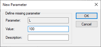
L =
0.1 λ = 0.1*1000 = 100 mm
d = 0.001λ = 0.001*1000 mm → 1 mm
g = =
0.001*1000 mm → 1 mm
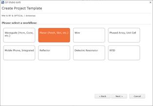
(1) Make a project template.
New Template, Microwaves & RF /
Optical, Anennas
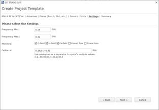
Create Project Template: Wire, Time
Domain
Units: default (mm, GHz)
Frequency Min. : 0.28
GHz
Frequency Max. : 0.32
GHz
Monitors: E-field, H-field, Farfield
Defined at: 0.3 GHz
Template name: short dipole
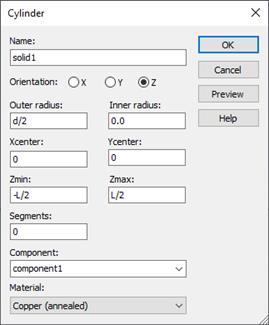
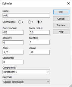
(2) Make a dipole antenna structure.
A. Make one short the dipole wire
using parameter symbols.
Modeling, Cylinder icon, ESC key,
Name: solid1, Orientation: Z
Outer radius: d/2, Inner radius: 0
X center:0 Y center:0
Z min:
-L/2 Z max : L/2
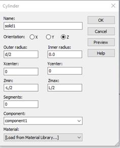
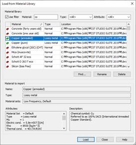
Material : Copper
(annealed)
Wire diameter: 0.001 wavelength

Dipole length: 0.1 wavelength
 +
+
Material: copper
Load from Material Library
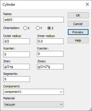
B. Make a
feed gap
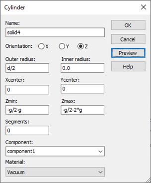
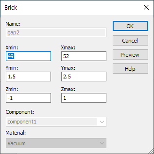
Modeling, Cylinder icon, ESC key,
Name: solid2, Orientation: Z
Outer radius: d/2, Inner radius: 0
X center:0 Y center:0
Z min:
-g/2 Z max : g/2
Material : Vacuum
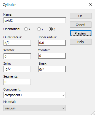
Feed gap: 0.001 wavelength

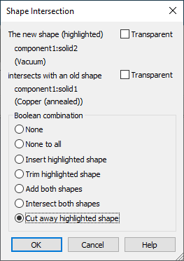
Ok
Shape intersection: Cut away
highlighted shape
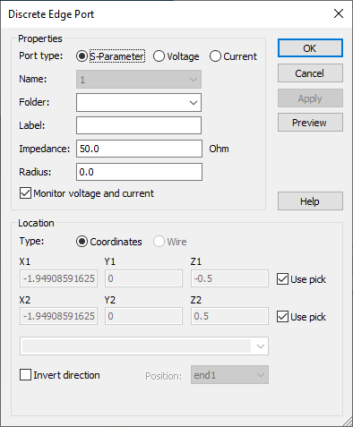
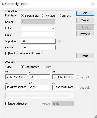
(3) Add an antenna source. Set up a
discrete port.
A. Specify the surfaces between which
a discrete port is to be applied.
Modeling
Picks, Pick Points, Pick Face Center
Place the mouse point on the one of gap faces and then
double click.
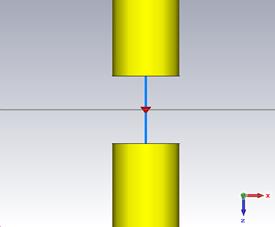
[Antenna Geometry]
(4) Simulate
Simulation, Setup Solver, Start
(5) Plot the geometry
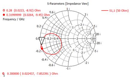
P2. Plot S11 on the Smith
chart. Plot |S11|(dB)
Cartesian.
1D Results, S-Parameters
RESULT TOOLS, 1D
Plot, Z Smith Chart
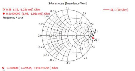
[Plot S11(dB)]
P3. Plot the real and imaginary parts of Z11.
1D Results, Z Matrix, Real and Imaginary
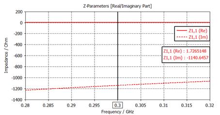
P4. Find the antenna input impedance Z11 at f0.
Z11의 Real/Imaginary plot에서 우클릭, Axis Maker, Pos.: 0.3
Axis Marker 주파수 (0.3 GHz)에서 표시되는 값 기록
ZA = ( 1.72 ) + j ( -1140 ) ohms
P5. Find the matching circuit element values (the first solution).
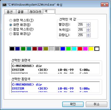
이론 부분의 ant-imped-match.exe 프로그램을 다운로드 후 실행
실행창 글꼴색, 바탕색 변경: 기본은 글꼴 백색, 바탕 흑색이라서 문서에 삽입하기 부적합
실행창 위 테두리에 커서 두고 우클릭
[속성], [색]
[화면 텍스트(T)] 선택 후 흑색 선택
[화면 배경(B)] 선택 후 백색 선택
ant-imped-match.exe을 실행하여 1st SOLUTION의 matching element 값 기록
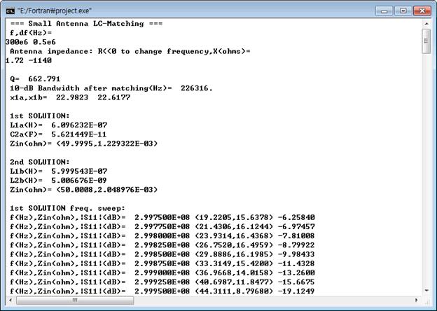
L = ( 0.609 ) uH
C = ( 56.2 ) pF
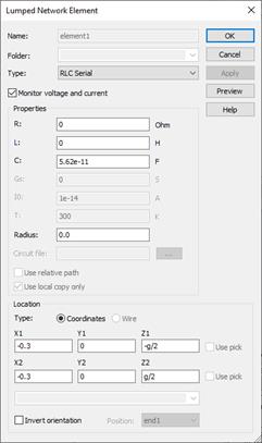
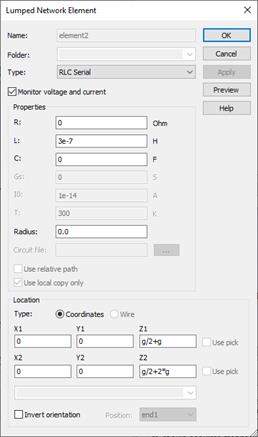
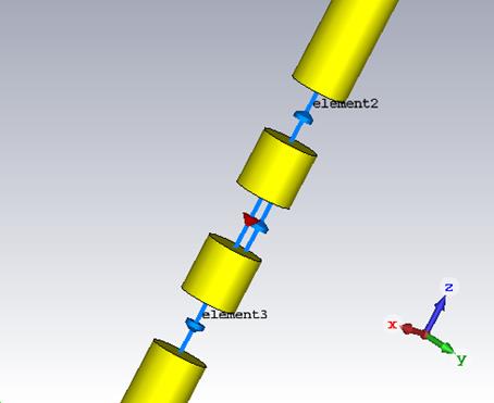
P6. Add matching circuit elements and simulate the structure. Plot S11 on the Smith chart.
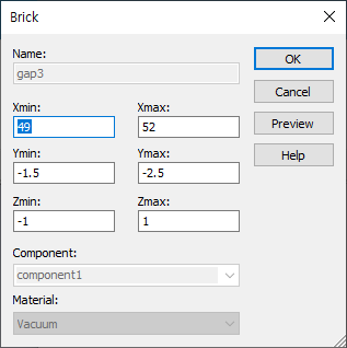
(1) 안테나 정합용 인덕터를 직렬로 연결하기 위한 gap을 다이폴에 생성
Ok
Shape intersection: Cut away
highlighted shape
Ok
Shape intersection: Cut away
highlighted shape
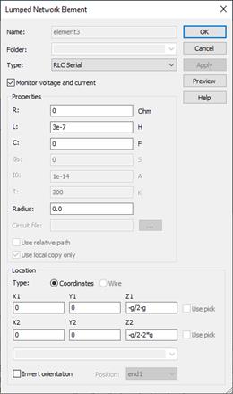
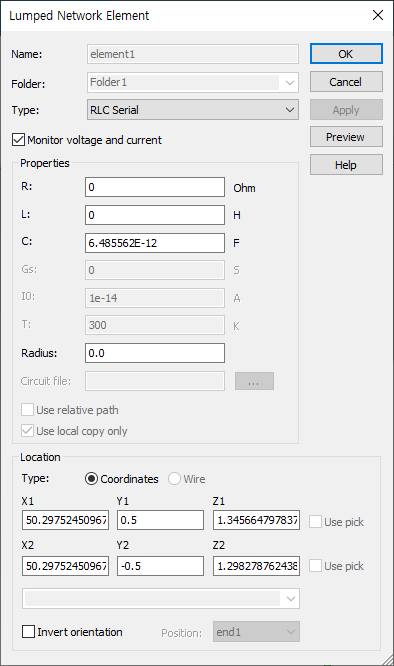
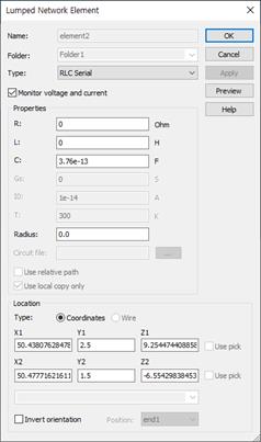
(2) 임피던스 정합 소자 연결
Navigation Tee, click the Lumped Elements, the right
mouse button
New lumped element
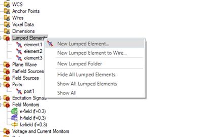
Element1 is C(Capacitor)
(3) Plot the antenna structure in a 3D form.
(4) Simulate
Simulation, Discrete Port
Simulation, Setup Solver, Start
(5) Plot S11
on the Smith chart.
1D Results, S-Parameters
RESULT TOOLS, 1D
Plot, Z Smith Chart
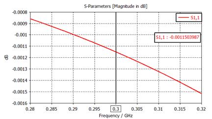
P7. Plot |S11|(dB) Cartesian after matching.
Find the 10-dB bandwidth
1D Results, S-Parameters
RESULT TOOLS, 1D
Plot, dB icon
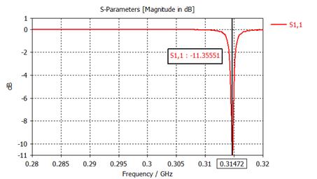
[10dB bandwith plot]
Plot |S11|(dB) at 0.31-0.32 GHz and use Measure Lines.
[Plot Here]
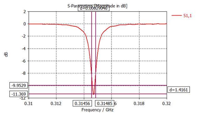
10-dB bandwidth = ( 0.29 ) MHz
10-dB bandwidth = ( 0.096 ) %
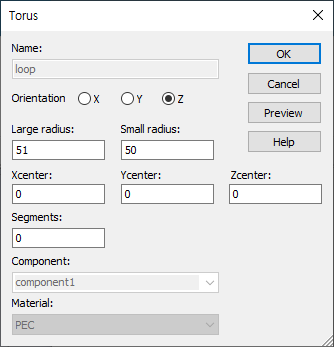
2. Small Loop
and Impedance Matching
Frequency: 300 MHz
Wavelength: 1 m
Loop diameter: 0.1 wavelength
Wire diameter: 0.001 wavelength
Feed gap: 0.001 wavelength
Wire material: coppper
All problems work at 300 MHz.
Simulation frequency range: 280-320 MHz
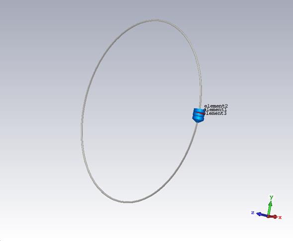
Figure: Small loop and impedance matching. Capacitors 2C1 are
inserted in the loop wire while the capacitor C2 is connected across
the feed gap in parallel with the discrete port.
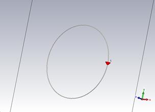
P1. Plot the antenna geometry
(방법: 구조 그리기)
1) 루프생성
Modeling, 고리 아이콘 선택, ESC 키, Name: solid1, Orientation: Z
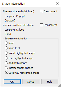
2) Feed gap 생성
Modeling, 직육면체 아이콘 선택, ESC 키, Name: solid2

Shape Intersection-> Cut away
highlighted shape
3) 포트설정
Modeling, Pick Points, Pick Face
Center, gap 한면에 마우스 위치후 더블클릭
Pick Points, Pick Face Center, gap 한면에 마우스 위치후 더블클릭
Simulation, Discrete Port
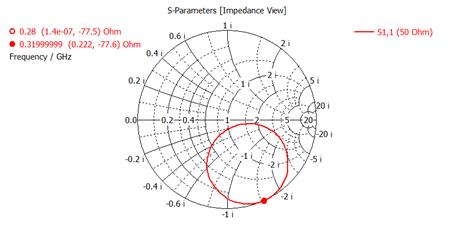
P2. Plot S11 on the Smith chart. Plot
|S11|(dB) Cartesian.
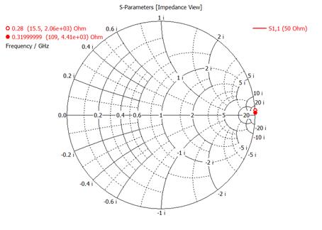
[Plot S11(dB)]
P3. Plot the real
and imaginary parts of Z11.
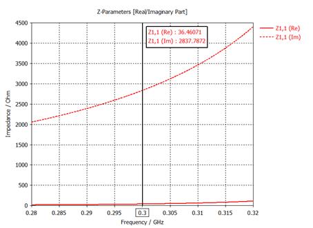
P4. Find the antenna
input impedance Z11 at f0.
ZA = ( 36 ) + j ( 2837 ) ohms
P5. Find the matching circuit
element values (the first solution).
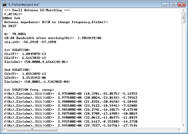
C1 = ( 0.188 ) pF
C2 = ( 6.62 ) pF
P6. Add matching circuit elements and simulate the structure. Plot the
antenna geometry. Plot S11 on the
Smith chart.
Modeling, Pick Points, Pick Face
Center, gap 한면에 마우스 위치후 더블클릭
Pick Points, Pick Face Center, gap 한면에 마우스 위치후 더블클릭
Simulation, Lumped Element
X1, X2 (-0.2)
X1, X2 (+0.2)
Modeling, 직육면체 아이콘 선택, ESC 키, Name: solid2
Shape Intersection-> Cut away
highlighted shape
Modeling, Pick Points, Pick Face
Center, gap 한면에 마우스 위치후 더블클릭
Pick Points, Pick Face Center, gap 한면에 마우스 위치후 더블클릭
Simulation, Lumped Element
Modeling, 직육면체 아이콘 선택, ESC 키, Name: solid2
Shape Intersection-> Cut away
highlighted shape
Modeling, Pick Points, Pick Face
Center, gap 한면에 마우스 위치후 더블클릭
Pick Points, Pick Face Center, gap 한면에 마우스 위치후 더블클릭
Simulation, Lumped Element

[Plot the antenna geometry]
P7. Plot |S11|(dB) Cartesian after matching.
Find the 10-dB bandwidth.
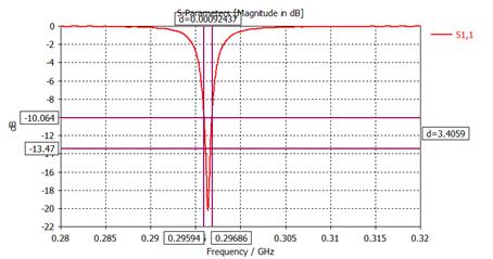
[10dB bandwith plot]
Plot |S11|(dB) at 0.29-0.30 GHz and use Measure Lines.
[Plot Here]
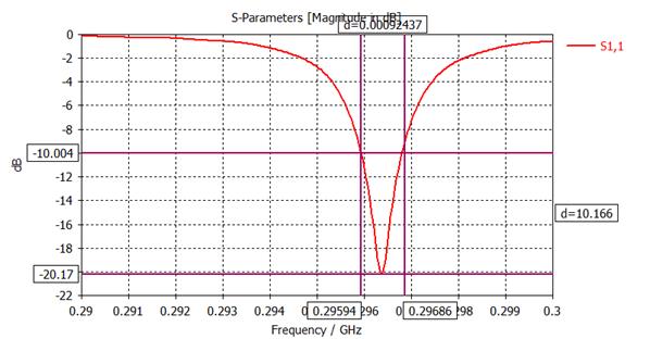
10-dB bandwidth = ( 0.9 ) MHz
10-dB bandwidth = ( 0.3 ) %