Antenna
Design
Lab
05 - Coupling Between Two Half-wave Dipoles
I. Simulation (70 points)
Make the
antenna structure
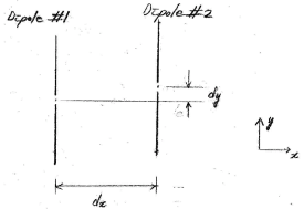
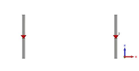
Dipole #1:
Antenna type: A center-fed
dipole with a circular cylindrical conductor
Design frequency: f
0 = (1000 + PIN/10) MHz
실습조교 PIN = 0000
Dipole end-to-end
length: L = 0.47 λ
Dipole diameter: d
= L/15
Dipole feed gap at the dipole
center: g = d
Frequency of
analysis: Centered at f0
Dipole axis: In z direction
Dipole material: PEC
Source: Discrete port (source
impedance = 50 ohms)
Frequency range: 0.5f0 to 1.5f0
Dipole #2:
Same as Dipole #1
Dipole
arrangement: dx = 1
wavelength at f0, dy = 0
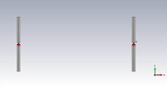
1. Plot the antenna structure in 3D.
2. Plot the reflection coefficient |S11|, |S12|, |S21|, |S22| (dB) of
the antenna on a same graph from 0.5f0
to 1.5 f0.
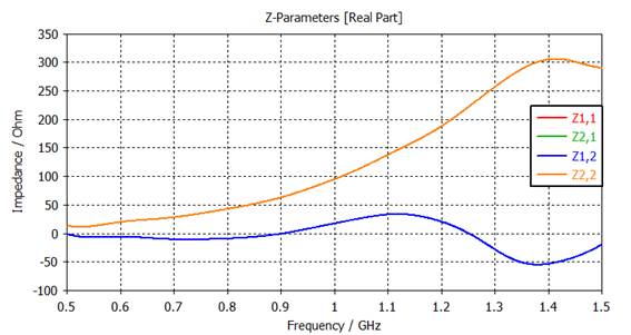
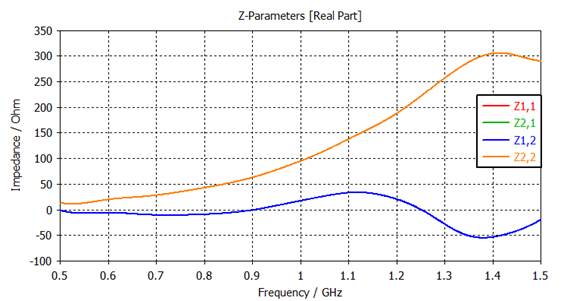
3. Plot R11, R21, R12, R22 of the antenan on a same graph from 0.5f0 to 1.5 f0.
4. Find R11, R21 at f0
using markers to read values.
5. Plot X11, X21, X12, X22 of the antenna on a same graph from 0.5f0 to 1.5 f0.
6. Find X11, X21 at f0
using markers to read values.
II. Discussions (30 points)
1. |S11|,
|S12|, |S21|, |S22| (dB) 그래프에서 |S12| = |S21|이 최대가 되는 주파수와 최소가 되는 주파수가 일치하는 지 확인하라.
2. Find the
input impedance of the Dipole #1 using
Z1,in = V1
/ I1 = Z11 -
(Z12)2 / (Z22 + Z2g)
Z2g
= 50 W
3. Find the antenna power
transfer ratio at f0 using
GT
= |S21|2
|S21|
(dB) = 20 log10 |S21|
4. 두 안테나가 서로 원거리에 있을 때 다음과 같은 Friis 전송방정식을 사용하여 안테나간의 전달전력을 구할 수 있다. 다음 식을 사용하여 안테나 간의 전력전달계수를 구하고 3에서의 값과 비교하라.
GT = P2 / P1
= (λ / 4πR)2 G1G2
R : 안테나간 거리
GT (dB) = 10 log10GT
G1 = D1 (1 - |S11|2)
: 안테나 1의 이득
G2 = D2 (1 - |S22|2)
: 안테나 2의 이득
D1, D2 : 두 안테나의 지향도
D1 = D2 = 1.6 (half-wave dipole gain)
Sample
Lab Report
I. Simulation
(70 points)
1. Plot the antenna structure in 3D.

2. Plot the reflection coefficient |S11|, |S12|, |S21|, |S22| (dB)
of the antenna on a same graph from 0.5f0 to 1.5 f0

3. Plot R11, R21, R12, R22 of the antenna on a same graph from 0.5f0 to
1.5 f0
4. Find R11, R21 at f0
using markers to read values.
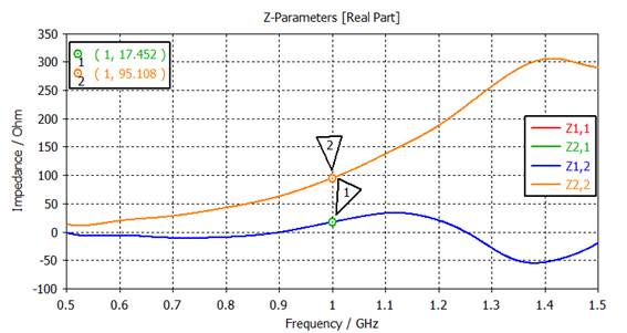
R11
= 95.1 W
R12
= 17.5 W
5. Plot X11, X21, X12, X22 of the antenna on a same graph from 0.5f0 to
1.5 f0.
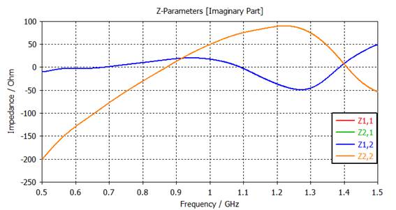
6. Find X11, X21 at f0
using markers to read values.
X11 =
49.1 W
X12 =
17.1 W
II. Discussions (30 points)
1. |S11|,
|S12|, |S21|, |S22| (dB) 그래프에서 |S12| = |S21|이 최대가 되는 주파수와 최소가 되는 주파수가 일치하는 지 확인하라.

|S12|는 |S11|이 최소가 되는 주파수 부근에서 최대가 된다.
2. Find the
input impedance of the Dipole #1 using
Z1,in = V1
/ I1 = Z11 -
(Z12)2 / (Z22 + Z2g)
Z2g
= 50 W
R11
= R22 = 95.1 W
R12
= R21 = 17.5 W
X11 = X22 = 49.1 W
X12 = X21 = 17.1 W
Z1,in = (R11 + j X11) -
(R12 + j X12)2 / (R22 + j X22 + Z2g)
= (95.1 +
j 49.1) - (17.5 + j 17.1)2 / (95.1 + j 49.1 + 50) = 93.7 +
j 45.4 W
3. Find the antenna
power transfer ratio at f0
GT = |S21|
(dB) = -19.5 dB at 1 GHz
4. 안테나 간의 전력전달계수
R = 1 λ
D1 = D2 = 1.6
|S11| = |S22| = -7.5 dB = 10(-7.5/20) = 0.421
G1 = G2 = 1.6 (1 - 0.4212) = 1.31
GT = (λ /
4πR)2 G1G2 = (1 / 4π)2×1.31×1.31 =
0.0109
GT (dB) = 10 log10GT = 10 log10
0.0109 = -19.6 dB
3의 값과 잘 일치한다.
CST
Studio Simulation 방법
I. Simulation
(70 points)
Make the
antenna structure
Dipole #1:
Antenna
type: A center-fed dipole with a circular cylindrical conductor
Design
frequency: f 0 = (1000 + PIN/1000)
MHz=1GHz
실습조교 PIN =
0000
Dipole
end-to-end length: L = 0.47 λ=141mm
Dipole
diameter: d = L/15=9.4 mm
Dipole
feed gap at the dipole center: g = d=9.4mm
Frequency
of analysis: Centered at f0
Dipole
axis: In z direction
Dipole
material: PEC
Source:
Discrete port (source impedance = 50 ohms)
Frequency
range: 0.5f0 to 1.5f0
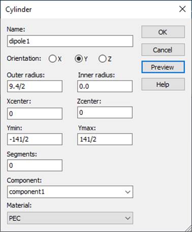
ㅇ 다이폴 #1 치수 계산
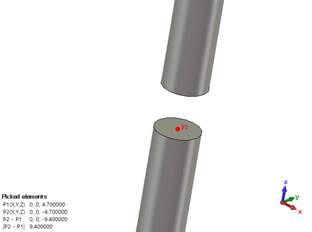
Dipole center at (x, y, z) =
(0, 0, 0)
Dipole axis: In y direction
PIN = 0000
f 0 =
(1000 + PIN/1000) MHz = 1GHz
λ = 300/1 = 300 mm
L = 0.1 λ =
0.47*300 = 141 mm
d = L/15 = 9.4 mm
g = d= 9.4mm
ㅇ 프로젝트 template 생성
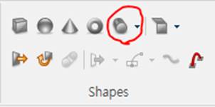
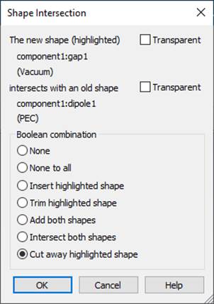
ㅇ 다이폴 #1 구조 그리기: 다이폴 원통 전체를 만든 후, 급전 간극 (feed gap)을 제거한다.
a) Modeling, Cylinder 아이콘 선택, ESC 키, Name: solid1, Orientation: Y
b)
Feed gap 생성
Modeling, Cylinder 아이콘 선택, ESC 키, Name: solid1, Orientation: Z
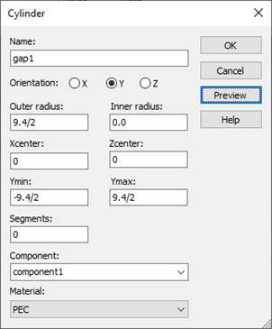
Next
Shape intersection: Cut away highlighted
shape
ㅇ 다이폴 #2 구조 그리기: 다이폴 #1을 복사한다.
Dipole #2:
Same as Dipole #1
Dipole
arrangement: dx = 1 wavelength at f0, dy =
0
dx =
λ = 300/1 = 300 mm
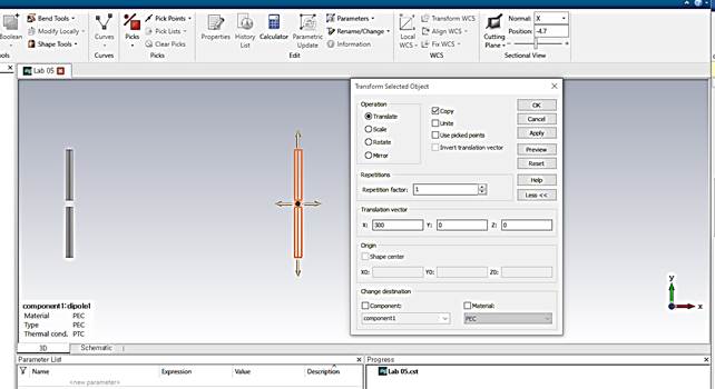
a) Select the dipole1
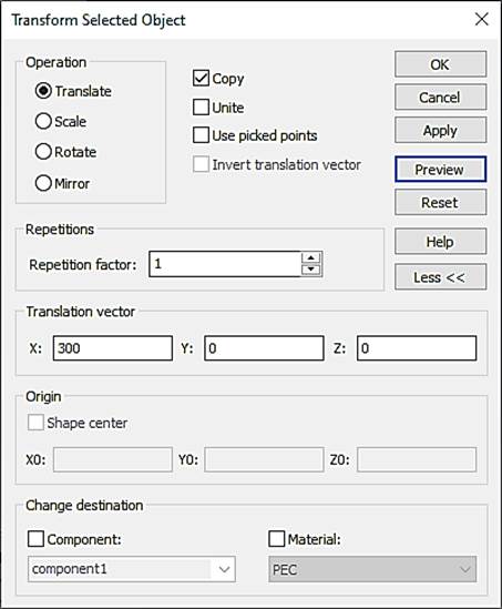
b) Choose the Modeling,
Transform
X: 300
Y: 0
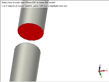
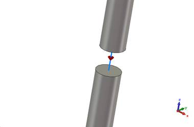
ㅇ 다이폴 급전 포트 설정
Modeling, Pick Points, Pick Face Center, gap 한면에 마우스 위치후 더블클릭
Pick Points, Pick Face Center, gap 한면에 마우스 위치후 더블클릭
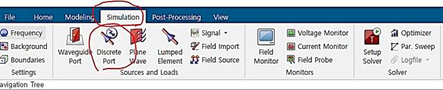
Simulation, Discrete Port
키보드 A를 누르고 중앙 선택
- 아래와 같이 점이 생성됨
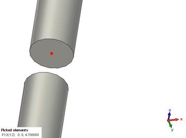
- 위와 같은 방식으로 반대쪽에도 점 생성
-
[Simulation]-[Discrete Port] Click
- 아래와 같은 창이 생성됨
- OK Click
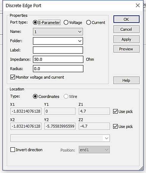
- 반대쪽도 똑같이 생성해주면 된다.
- 유의할 점은 포트의 방향은 같아야 한다는 것.
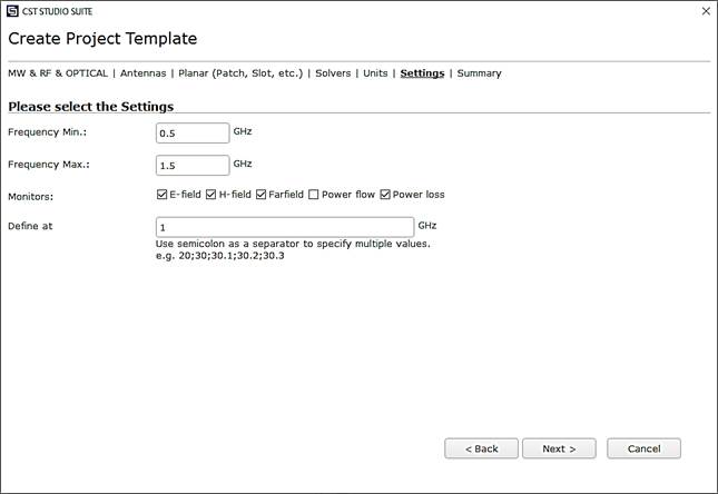
ㅇ 시뮬레이션 설정
주파수 설정:
Simulation, Frequency, Min. frequency: 0.5,
Max. frequency: 1
필드 모니터 설정:
Simulation, Field Monitor, E-field,
Frequency, Frequency:1, Apply
Simulation, Field Monitor, H-field and
Surface current, Frequency, Frequency:1, Apply
Simulation, Field Monitor, Far field/RCS,
Frequency, Frequency:1, Apply
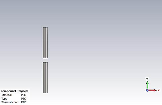
1. Plot the antenna structure in 3D.
2. Plot the reflection coefficient |S11|, |S12|, |S21|, |S22| (dB)
of the antenna on a same graph from 0.5f0 to 1.5 f0
Navigation Tree, 1D Results, S-Parameters
RESULT TOOLS - 1D Plot, dB
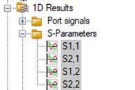
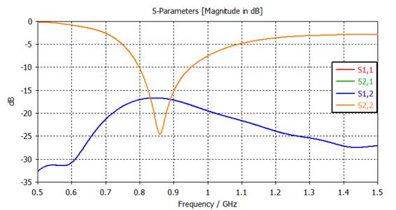
S1,1과 S2,2는 동일하므로 겹쳐서 그려짐.
S1,2와 S2,1은 동일하므로 겹쳐서 그려짐.
3. Plot R11, R21, R12, R22 of the antenna on a same graph from 0.5f0 to
1.5 f0
Navigation Tree, 1D Results, Z-Parameters,
Select All

1D Plot, Real
4. Find R11, R21 at f0
using markers to read values.
- 마우스 우클릭, [Add Curve Marker]
- 이후 원하는 선에 더블 클릭해주면 마커가 생성됨
- 마커를 더블 클릭하면 원하는 주파수 선택가능
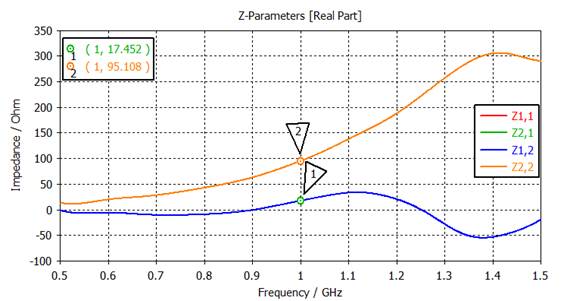
R11
= 95.1 W
R12
= 17.5 W
5. Plot X11, X21, X12, X22 of the antenna on a same graph from 0.5f0 to
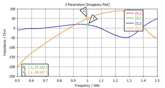
1.5 f0.
Navigation Tree, 1D Results, Z-Parameters,
Select All
1D Plot, Imaginary
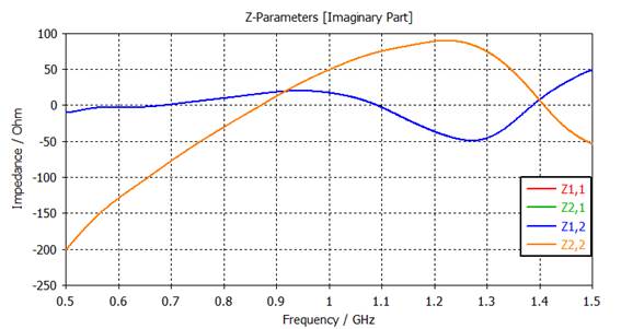
6. Find X11, X21 at f0
using markers to read values.

X11 =
49.1 W
X12 =
17.1 W